

Departments
 Integrated Circuits
Need Help
Home >
Integrated Circuits >
Special Function >
Analog Devices
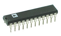
AD7537 Dual 12-Bit DAC Datasheet
Photograph
Features
- Two 12-Bit DACs in One Package
- DAC Ladder Resistance Matching: 0.5%
- 4-Quadrant Multiplication
- Low Gain Error (1 LSB max Over Temperature)
- Byte Loading Structure
- Fast Interface Timing
Pin Layout

Pin Description
| Pin Number | Description |
|---|---|
| 1 | AGNDA - Analogue Ground for DAC A |
| 2 | Iouta - Current Output DAC A |
| 3 | Rfba - Feedback Resistor DAC A |
| 4 | Vrefa - Voltage Reference DAC A |
| 5 | CS - Chip Select (Active Low) |
| 6 | DB0 - Data Input Bit 0 |
| 7 | DB1 - Data Input Bit 1 |
| 8 | DB2 - Data Input Bit 2 |
| 9 | DB3 - Data Input Bit 3 |
| 10 | DB4 - Data Input Bit 4 |
| 11 | DB5 - Data Input Bit 5 |
| 12 | DGND - Digital Ground |
| 13 | DB6 - Data Input Bit 6 |
| 14 | DB7 - Data Input Bit 7 |
| 15 | A0 - Address Line 0 |
| 16 | A1 - Address Line 1 |
| 17 | CLR - Clear Input (Active Low) |
| 18 | WR - Write Input (Active Low) |
| 19 | UPD - Update DAC Register |
| 20 | Vdd - Positive Supply |
| 21 | Vrefb - Reference Input to DAC B |
| 22 | Rfbb - Feedback Resistor for DAC B |
| 23 | Ioutb - Current Output Terminal of DAC B |
| 24 | AGNDB - Analog Ground for DAC B |
Dimensional Drawing
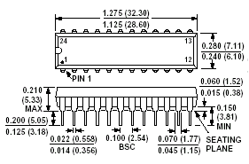
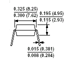
Technical Data