

Departments
 Integrated Circuits
Need Help
Home >
Integrated Circuits >
Special Function >
Analog Devices
AD7528 CMOS Dual 8-Bit Buffered Multiplying DAC Datasheet
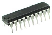
Photograph
Features
- On-Chip Latches for Both DACs
- +5 V to +15 V Operation
- DACs Matched to 1%
- Four Quadrant Multiplication
- TTL/CMOS Compatible
- Latch Free (Protection Schottkys not Required)
Pin Layout

Pin Description
| Pin Number | Description |
|---|---|
| 1 | AGND - Analog Ground |
| 2 | OUTA - Output A |
| 3 | RfbA - Resistor Feedback A |
| 4 | Vrefa - Voltage Reference A |
| 5 | GND - Ground |
| 6 | DAC A/B - DAC A/B Select |
| 7 | DB7 - Data Inputs DB7 |
| 8 | DB6 - Data Inputs DB6 |
| 9 | DB5 - Data Inputs DB5 |
| 10 | DB4 - Data Inputs DB4 |
| 11 | DB3 - Data Inputs DB3 |
| 12 | DB2 - Data Inputs DB2 |
| 13 | DB1 - Data Inputs DB1 |
| 14 | DB0 - Data Inputs DB0 |
| 15 | CS - Chip Select |
| 16 | WR - Write |
| 17 | Vdd - Positive Supply |
| 18 | Vrefb - Voltage Reference B |
| 19 | Rfb - Resistor Feedback |
| 20 | OUTB - Output B |
Dimensional Drawing


Technical Data