
PCB Manufacturing Technical Information
|
|
||||||||||||||||||||||||||||||||||||||
|
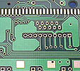
Track Sizes Careful consideration of the current passing through the track needs to be made prior to determining the track size. |
||||||||||||||||||||||||||||||||||||||
|
Minimum Track Width: 10 mil Minimum Track Clearance: 10 mil |
||||||||||||||||||||||||||||||||||||||
|
Pad Sizes Pad sizes are determined by the size of the lead or device to be inserted in the hole, the larger the device leg the larger the pad, this will secure the device and prevent damage to the board or trackes if the device is moved while fixed to the board. |
||||||||||||||||||||||||||||||||||||||
|
Minimum Pad Size: Hole Size + 20 mil Minimum Pad Clearance: 10 mil Minimum Pad Size for VIA: 40 mil with a Hole Size of 20 mil Recommended Pad Size for Resistor/Capacitor: 62 mil with a Hole Size of 36 mil |
||||||||||||||||||||||||||||||||||||||
|
Hole Sizes Using the standard drill sizes as below, will ensure your board is produced quickly and accurately, |
||||||||||||||||||||||||||||||||||||||
|
Minimum Hole Size: 0.6 mm Maximum Hole Size: 6.6 mm Standard Drill Sizes: |
||||||||||||||||||||||||||||||||||||||
|
||||||||||||||||||||||||||||||||||||||
|
Font The same font used throughout the board layout provides a professional and neat appearance on your board, |
||||||||||||||||||||||||||||||||||||||
|
Standard Font: Sans Serif |
||||||||||||||||||||||||||||||||||||||
|
Material A number of different board materials are available, our standard is |
||||||||||||||||||||||||||||||||||||||
|
Standard Material: FR4 width 1.6mm, Board Width of 0.8mm is available on request |
||||||||||||||||||||||||||||||||||||||
 The following specifications define the requirements for single sided and double sided PCBs to be submitted to our
production department. These requirements can be easily checked using your
pcb program and the various tools included with the program,
The following specifications define the requirements for single sided and double sided PCBs to be submitted to our
production department. These requirements can be easily checked using your
pcb program and the various tools included with the program,