

Departments
 Integrated Circuits
Need Help
Home > Integrated Circuits > Special Function > Analog Devices
AD9501 Digitally Programmable Delay Generator Datasheet
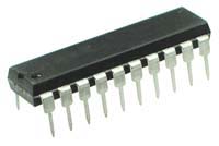
Photograph
Features
- Single +5V Supply
- TTL and CMOS Compatible
- 10ps Delay Resolution
- 2.5ns to 10µs Full Scale Range
- Maximum Trigger Rate 50MHz
Pin Layout

Pin Description
| Pin Number | Description |
|---|---|
| 1 | +Vs - Positive Supply |
| 2 | LATCH - Latch Data Input |
| 3 | TRIGGER - Start Conversion |
| 4 | RESET - Output Reset |
| 5 | DAC OUT - Analog Output |
| 6 | Cext - External Capacitor for Full Scale Delay Range |
| 7 | Rset - Full Scale Delay Range |
| 8 | OFFSET ADJUST - See Datasheet |
| 9 | GND - Ground |
| 10 | OUT - Delayed Output Pulse |
| 11 | +Vs - Positive Supply |
| 12 | D0 - Data input Bit 0 |
| 13 | D1 - Data Input Bit 1 |
| 14 | D2 - Data Input Bit 2 |
| 15 | D3 - Data Input Bit 3 |
| 16 | D4 - Data Input Bit 4 |
| 17 | D5 - Data Input Bit 5 |
| 18 | D6 - Data Input Bit 6 |
| 19 | D7 - Data Input Bit 7 (MSB) |
| 20 | GND - Ground |
Dimensional Drawing


Technical Data