

Departments
 Integrated Circuits
Need Help
Home >
Integrated Circuits >
Special Function >
Analog Devices
AD7712 Signal Conditioning ADC Datasheet
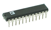
Photograph
Features
- Charge Balancing ADC
- - 24 Bits No Missing Codes
- - ±0.0015% Nonlinearity
- Programmable Gain for Both Inputs
- - Gains from 1 to 128
- - Differential Input for Low Level Channel
- High Level and Low Level Analog Input Channels
- Low-Pass Filter with Programmable Filter Cutoffs
- Ability to Read/Write Calibration Coefficients
- Bidirectional Microcontroller Serial Interface
- Internal/External Reference Option
- Single or Dual Supply Operation
- Low Power (25mW typ) with Power-Down Mode (100µW typ)
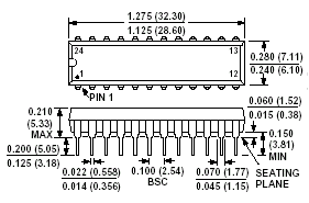
Pin Layout

Pin Description
| Pin Number | Description |
|---|---|
| 1 | SCLK - Serial Clock |
| 2 | MCLK IN - Master Clock In |
| 3 | MCLK OUT - Master Clock Out |
| 4 | A0 - Address Input |
| 5 | SYNC - Synchronization (Active Low) |
| 6 | MODE - Clocking Mode |
| 7 | +AIN1 - Analog Input Channel 1 |
| 8 | -AIN1 - Analog Input Channel 1 |
| 9 | STANDBY - Logic Input (Active Low) |
| 10 | TP - Test Pin |
| 11 | Vss - Analog Negative Supply |
| 12 | AVdd - Analog Positive Supply |
| 13 | Vbias - Input Bias Voltage |
| 14 | REF IN- - Reference Input |
| 15 | REF IN+ - Reference Input |
| 16 | REF OUT - Reference Output |
| 17 | AIN2 - Analog Input Channel 2 |
| 18 | AGND - Analog Ground |
| 19 | TFS - Transmit Frame Synchronization (Active Low) |
| 20 | RFS - Receive Frame Synchronization (Active Low) |
| 21 | DRDY - Logic Output (Active Low) |
| 22 | SDATA - Serial Data |
| 23 | DVdd - Digital Positive Supply |
| 24 | DGND - Digital Ground |
Dimensional Drawing
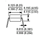
Technical Data