

Departments
 Integrated Circuits
Need Help
Home >
Integrated Circuits >
74 Series >
74 Series
7474 - 7474 Dual D Flip-Flop Datasheet
Photograph

Features
- Two D-Type Flip-Flops
- Outputs Directly Interface to CMOS, NMOS and TTL
- Large Operating Voltage Range
- Wide Operating Conditions
- Not Recommended for New Designs Use 74LS Series - 74LS74 IC
Pin Layout
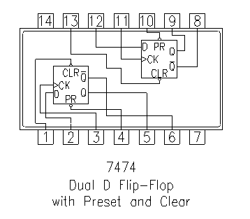
Pin Description
| Pin Number | Description |
|---|---|
| 1 | Clear 1 Input |
| 2 | D1 Input |
| 3 | Clock 1 Input |
| 4 | Preset 1 Input |
| 5 | Q1 Output |
| 6 | Complement Q1 Output |
| 7 | Ground |
| 8 | Complement Q2 Output |
| 9 | Q2 Output |
| 10 | Preset 2 Input |
| 11 | Clock 2 Input |
| 12 | D2 Input |
| 13 | Clear 2 Input |
| 14 | Positive Supply |
Dimensional Drawing

Technical Data
Absolute Maximum Ratings
| Supply Voltage | 7V |
| Input Voltage | 5.5V |
| Operating Free Air Temperature | 0°C to +70°C |
| Storage Temperature Range | -65°C to +150°C |
Recommended Operating Conditions
| Symbol | Parameter | Min | Typ | Max | Units |
|---|---|---|---|---|---|
| Vcc | Supply Voltage | 4.75 | 5 | 5.25 | V |
| Vih | HIGH Level Input Voltage | 2 | V | ||
| Vil | LOW Level Input Voltage | 0.8 | V | ||
| Ioh | HIGH Level Output Current | -0.4 | mA | ||
| Iol | LOW Level Output Current | 16 | mA | ||
| Ta | Free Air Operating Temperature | 0 | 70 | °C |
Electrical Characteristics
| Symbol | Parameter | Conditions | Min | Typ | Max | Units |
|---|---|---|---|---|---|---|
| Vi | Input Clamp Voltage | Vcc=Min Ii=-12mA | -1.5 | V | ||
| Voh | HIGH Level Output Voltage | Vcc=Min Ioh=MAX Vil=MAX | 2.4 | 3.4 | V | |
| Vol | LOW Level Output Voltage | Vcc=Min Iol=MAX Vih=MAX | 0.2 | 0.4 | V | |
| Ii | Input Current@MAX Input Voltage | Vcc=Max Vi=5.5V | 1 | mA | ||
| Iih | HIGH Level Input Current | Vcc=Max Vi=2.4V | 40 | µA | ||
| Iil | LOW Level Input Current | Vcc=Max Vi=0.4V | -1.6 | mA | ||
| Ios | Short Circuit Output Current | Vcc=Max | -18 | -55 | mA | |
| Icch | Supply Current with Outputs HIGH | Vcc=Max | 4 | 8 | mA | |
| Iccl | Supply Current with Outputs LOW | Vcc=Max | 12 | 22 | mA |
Switching Characteristics at Vcc=5V,Ta=25°C
| Symbol | Parameter | Conditions | Min | Typ | Max | Units |
|---|---|---|---|---|---|---|
| tplh | Propagation Delay Time LOW-to-HIGH Level Output | Cl=15pF Rl=400R | 22 | nS | ||
| tphl | Propagation Delay Time HIGH-to-LOW Level Output | Cl=15pF Rl=400R | 15 | nS |